
Full specifications are available in the MP7 userguide. The latest version of which may be found here.
| Part | Component options |
|---|---|
| FPGA |
Xilinx Virtex-7 XC7VX415T Xilinx Virtex-7 XC7VX485T Xilinx Virtex-7 XC7VX550T Xilinx Virtex-7 XC7VX690T |
| Optical Transceivers |
Transmitter - Avago Technologies MiniPOD AFBR-81uVxyZ Receiver - Avago Technologies MiniPOD AFBR-82uVxyZ |
| Optical Interface | Sylex {3xPRIZM-MTP(M)36F OM3 36F 17cm} |
| General purpose I/O | Samtec 0.4mm Super Low Profile Socket Strip SS4-50 |
| Form factor | μTCA |
| QDR SRAM |
Cypress CY7C2163KV18-550BZXI Cypress CY7C2263KV18-550BZXI Cypress CY7C25632KV18-550BZXI Cypress CY7C2663KV18-550BZXC |
| MMC-Controller | Atmel AT32-UC3A-3256 |
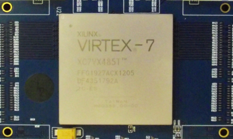
The processing in the MP7 is performed by the high-performance Xilinx Virtex-7, FPGA, endowing the MP7 with powerful computational abilities and a high data throughput.
The core Firmware in the MP7 is designed to control the operation of the board, minimising the work required by the user.
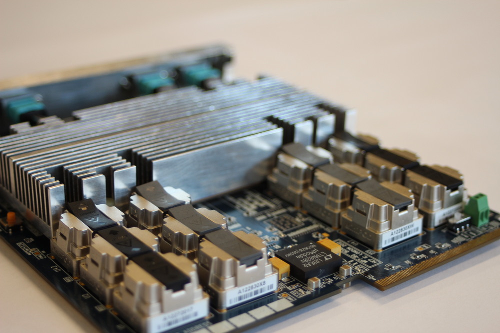
The large data processing I/O requirements of the MP7 are met by its optical interface, provided by up to six Avago MiniPOD transmitters and six receivers. Designed for the super-computing industry each provides 12 optical links running at up to 10.3 Gbps, giving the MP7 a total optical bandwidth of up to 740 Gbps in each direction.
The single interface of the MP7 for the sending and receiving data offers several distinct advantages. The primary advantage is that the board ceases to have a specific role and becomes a truly generic stream-processing engine, the application of the board to a specific task is therefore no longer restricted by the bandwidth and compatibility of each type of interface, but only by the total bandwidth, whilst all specialisation required for a task is contained within the programming of the board and the interconnections between boards.
The large number of high-speed optical links in the MP7 presents a significant design challenge and have therefore been rigorously validated by loop-back tests. Running the links at 10 Gbps the MP7 transfers 0.48 Tbps in each direction. To date, the MP7s have transferred in excess of an Exabit of data without an observed error, giving a limit on the per-board bit-error rate of approximately 3 × 10-17.
The front-panel optical connections are four industry-standard, 48-way MTP connectors of which 36-channels on each connector are utilised. All channels within each MTP carry data in the same direction. The interface to external fibres is via MTP-MTP adaptors which are mounted on the front-panel of the board.
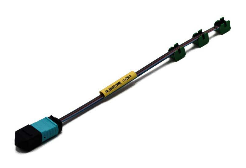
To acheive their small footprint and high data-density, Avago MiniPODs use PRIZM LightTurn connectors for their optical interface. The transition from PRIZM LightTurn connectors to MTP-48 is provided by four Sylex {3xPRIZM-MTP(M)36F OM3 36F 17cm} assemblies utilizing unpeelable ribbon, minimizing the risk of damage in the high airflow μTCA-environment.
The MP7 provides two general-purpose interfaces via the AMC card-edge connector, including 7 general-purpose LVDS pairs, and low-profile connectors on the top-face of the board which may be used as front-panel I/O. The Select-I/O resources on the Virtex-7 FPGA allow each differential pair to run at speeds of up to 1.866 Gbps. Other connectors include an AMC card-edge connector, which features differential connections, as well as Telecoms Clock-A, Fabric Clock-A, geographic addressing, IPMI and JTAG.
Due the high-performance processing required of the MP7, fast memory is demanded. The MP7 provides up to 288Mbit of QDR II+ SRAM in the form of 2×144Mbit Cypress (8M×18bit) chips, giving memory access of up to 550MHz DDR (1100MHz). The SRAM chosen is pin-compatible with lower-capacity parts and so cost and performance may be balanced.
The MP7 has LVDS clock inputs from AMC card-edge connections TCLKA, FCLKA and TCLKC. The FCLKA is available for use as a PCIe clock, as well as for distribution of the LHC machine clock from an AMC13 card located in the redundant slot of a standard dual star μTCA crate. Any of the clocks may be passed through a Silcon Labs SI5326 jitter attenuator which can also act in a standalone frequency synthesis mode. The MP7 also accepts a clock input through the front panel on a pair of Samtec SMP-EM - 50 Ohm SMP RF Plug connectors.
The MP7 implements MMC functionality using an Atmel AT32-UC3A-3256. The microcontroller implements IPMI communications, management and monitoring of the μTCA extraction handle, the temperature and humidity sensors and the μTCA indicator LEDS. The microcontroller also provides a USB-2 interface to the board, a serial console and sets the IP-address of the board. The USB connector on the MP7 is a micro-B type connector so that it fits on the bottom face of the board.
Systems monitoring is particularly important on the MP7 because of the board's extreme performance and the complexity of, and tight requirements placed on, the power supply network. Current and Temperature Monitors are used to monitor:
- Temperature, output-voltage and current-draw on each of the switch mode regulators
- Temperature inside the FPGA
- SRAM termination voltages
It has been suggested that the primary cause of the failure of optical components in the ATLAS experiment may be the humidity of the operating environment (Weidberg, T. 2011) and that the same may apply to optical failures seen by CMS. Given the high density of optics on the MP7, a humidity and temperature sensor is used to monitor atmospheric humidity.